Skip to content
Skip to content
Call Us for more Information: 8757870948
Email Us: swiftlysewa@gmail.com
Login/Register
First 20 students get 50% discount .
swiftlysewa career portalswiftlysewa career portal
  • Category
    • 3 week
    • Android App Dev
    • Anysys
    • Artificial Intelligence
    • CAD & CAM
    • Construction & Structural Engineering
    • CSE Special Courses
    • Data Science
    • Design and Analysys
    • DIPLOMA
    • DSA with Python programming
    • engineering
    • Ethetical Hacking
    • Fundamentals of Robotics
    • Graphic Design
  • Home
    • User Register
    • User Login
    • Dashboard
    • About
    • Download App
  • All Courses
  • All Instructors
  • Internships
  • Pages
    • Live Meeting/Clases
    • Events
    • Certificate verifications
    • About
    • Refund and Returns Policy
    • My account
      • Instructor Registration
      • User Register
      • FAQs
    • Contact Us
    • Download App
  • Dashboard
0

Currently Empty: ₹0.00

Continue shopping

swiftlysewa career portalswiftlysewa career portal
  • Home
    • User Register
    • User Login
    • Dashboard
    • About
    • Download App
  • All Courses
  • All Instructors
  • Internships
  • Pages
    • Live Meeting/Clases
    • Events
    • Certificate verifications
    • About
    • Refund and Returns Policy
    • My account
      • Instructor Registration
      • User Register
      • FAQs
    • Contact Us
    • Download App
  • Dashboard
  • Home
  • Course
  • PCB Design 3-WEEK

PCB Design 3-WEEK

  • By Shankar kumar
  • PCB Design
  • (0 Rating)
Breadcrumb Abstract Shape
  • Course Info
  • Instructor
  • Reviews
  • More
    • The PCB Design Course is designed to help learners understand the fundamental to advanced concepts of Printed Circuit Board (PCB) designing. This course provides a complete roadmap for creating efficient, reliable, and industry-standard PCBs using modern design tools. Whether you are a beginner or someone looking to improve your electronics design skills, this course will help you build the confidence to design real-world PCB projects.


      ✨ What You Will Learn

      • Basics of PCB: Understanding components, circuits, layers, and board types.

      • Schematic Design: How to draw clean, professional schematics for any circuit.

      • PCB Layout Techniques: Component placement, routing, vias, and ground planes.

      • Design Tools: Hands-on training with popular tools like Eagle, KiCAD, or Altium Designer.

      • Signal Integrity: High-speed routing, EMI/EMC basics, and noise reduction.

      • 3D Visualization: How to preview and verify your PCB in 3D before printing.

      • Fabrication Process: Understanding Gerber files, PCB layers, and manufacturing guidelines.

      • Real-World Projects: Designing PCBs for Arduino modules, sensor boards, power circuits, and more.


      🎯 Course Outcomes

      By the end of the course, you will be able to:

      • Design professional, multi-layer PCBs with confidence

      • Create schematics and convert them into manufacturable designs

      • Optimize PCB layout for performance and durability

      • Prepare files and communicate with PCB manufacturers

      • Build and test your own electronic products


      👨‍🏫 Who Should Take This Course?

      • Electronics & Electrical Engineering students

      • IoT and Embedded systems enthusiasts

      • Hobbyists who love designing circuits

      • Start-up founders building hardware products

      • Anyone interested in PCB design from scratch

      Show More
      What Will You Learn?
      • You learn basic to advance labels PCB Design.

      Material Includes

      • You learn basic to advance labels PCB Design.
      • You get a internship certificate.

      Requirements

      • A laptop or phone and good internet connection.

      Audience

      • Student and working professional.

      Course Content

      Chapter 1
      Chapter 1 lays the foundation for understanding the world of Printed Circuit Boards (PCBs). This chapter introduces you to the basic concepts, structure, and purpose of PCBs, explaining how they serve as the backbone of all modern electronic devices. You will learn why PCBs are used, how they replaced traditional wiring methods, and what makes them essential for creating compact, reliable, and efficient circuits. This chapter also explains the different types of PCBs, their layers, materials, and common components you will encounter throughout the course. You will explore the anatomy of a PCB — including copper traces, pads, vias, solder masks, and silkscreen — gaining the visual understanding needed for future design work. By the end of Chapter 1, learners will have a solid grasp of PCB basics, circuit flow, and the terminologies used in PCB engineering, setting a strong foundation for schematic creation and layout design in the upcoming chapters.

      • Chapter 1
        05:23
      • PCB Design Quiz on Chapter 1

      Chapter 2
      📘 Chapter 2: Understanding Electronic Components & Schematic Design Chapter 2 takes you deeper into the core of PCB development by introducing electronic components and the process of creating professional schematic diagrams. This chapter explains how different components—such as resistors, capacitors, diodes, ICs, LEDs, transistors, sensors, and connectors—are represented symbolically in a schematic and how they behave in a circuit. You will learn the importance of component selection, reading datasheets, understanding pin configurations, and mapping components correctly. The chapter also focuses on building clean, error-free schematics, teaching you best practices for labeling, net connections, hierarchy, and avoiding common design mistakes. Through practical examples, learners will understand how to convert a circuit idea into an accurate schematic that can later be transformed into a PCB layout. This chapter sets the stage for mastering the essential workflow of PCB design, ensuring that your future layouts are precise, organized, and ready for manufacturing.

      • Chapter 2
        10:56
      • PCB Design Quiz on Chapter 2

      Chapter 3
      📘 Chapter 3: PCB Layout Design – Component Placement & Routing Chapter 3 is one of the most important stages in PCB Design, where your schematic is transformed into a physical board layout. In this chapter, you will learn how to strategically place components on the PCB to ensure optimal performance, easy routing, and professional quality. You’ll understand placement rules, spacing requirements, and how to organize components based on function, signal flow, and design constraints. The chapter also introduces you to routing techniques, including single-layer, double-layer, and multilayer routing strategies. You will learn how to create clean copper traces, use vias effectively, and avoid common problems like signal noise, crosstalk, and incorrect routing angles. Special focus is given to power routing, ground planes, trace width selection, and best practices for creating stable and reliable connections. By the end of Chapter 3, you will have the skills to convert a schematic into an optimized PCB layout ready for 3D viewing and pre-manufacturing checks. This chapter builds the confidence to design real-world PCBs that are efficient, safe, and professionally structured.

      • Chapter 3
        14:38
      • PCB Design Quiz on Chapter 3

      Chapter 4
      📘 Chapter 4: Design Rules, Validation & Preparing for Manufacturing Chapter 4 focuses on the crucial step of ensuring your PCB design meets industry standards and is fully ready for fabrication. You will learn about Design Rule Checks (DRC) and Electrical Rule Checks (ERC), which help you identify and correct mistakes such as spacing errors, unconnected nets, incorrect trace widths, and component clearance issues. This chapter explains how PCB design software uses these rules to validate your layout and ensure your board functions safely and reliably. You’ll also explore essential manufacturing considerations—such as copper thickness, minimum drill sizes, solder mask clearances, and silkscreen guidelines—to make sure your PCB can be produced without errors. The chapter teaches you how to generate Gerber files, drill files, and assembly files, which are the standard formats required by PCB fabrication companies. By the end of Chapter 4, you will be fully capable of validating your design, fixing critical errors, and exporting all necessary files for professional PCB manufacturing. This chapter ensures your design transitions smoothly from digital layout to real, production-ready hardware.

      • Chapter 4
        13:30
      • PCB Design Quiz on Chapter 4

      Chapter 5
      📘 Chapter 5: PCB Fabrication, Assembly & Final Testing Chapter 5 takes you through the final and most exciting stage of the PCB design journey — turning your digital layout into a real, functioning circuit board. This chapter explains the entire PCB fabrication process, from layer creation and copper etching to drilling, plating, solder masking, and finishing. You’ll understand how manufacturers convert your Gerber files into physical boards and the quality checks involved at each stage. Next, the chapter covers PCB assembly, where components are placed and soldered onto the board. You will learn about SMT (Surface Mount Technology), THT (Through-Hole Technology), reflow soldering, wave soldering, and how assembly houses ensure precision and reliability. Finally, the chapter concludes with testing and troubleshooting. You will explore continuity testing, visual inspection, automated optical inspection (AOI), functional testing, and ways to detect common issues like shorts, cold solder joints, and component misplacements. By the end of Chapter 5, you will have a complete understanding of how PCBs are manufactured, assembled, tested, and prepared for real-world applications—making you fully confident to design and build your own hardware products from start to finish.

      • Chapter 5
        11:49
      • PCB Design Quiz on Lecture 5

      Tags

      • DESIGN

      A course by

      Shankar kumar
      Shankar kumar
      AI Engineer

      Student Ratings & Reviews

      No Review Yet
      No Review Yet

      Course Includes:

      • Price:
        ₹1,000.00 Original price was: ₹1,000.00.₹249.00Current price is: ₹249.00.
      • Instructor:Shankar kumar
      • Duration: 20 hours
      • Lessons:5
      • Students:1
      • Level:All Levels
      ₹249.00 ₹1,000.00
      Wishlist
      Hi, Welcome back!
      Forgot Password?
      Don't have an account?  Register Now

      Share On:

      Courses You May Like

      ChatGPT Image Jan 13, 2026, 07_39_34 PM
      20 hours
      All Levels
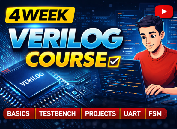
      Verilog HDL 4-Week
      (5.0/ 1 Rating)
      ₹900.00 Original price was: ₹900.00.₹249.00Current price is: ₹249.00.
      • 5 Lessons
      • 6 Students
      All Levels
      Verilog HDL 4-Week
      (5.0/ 1 Rating)
      ₹900.00 Original price was: ₹900.00.₹249.00Current price is: ₹249.00.

      This 4-Week Verilog HDL Course is designed to build strong foundations in digital system design and hardware description using Verilog. The course focuses on hands-on...

      • 5 Lessons
      • 6 Students
      Enroll Now
      cropped-Gold-and-Maroon-Vibrant-Diwali-Festival-Sale-Marketing-Instagram-Post-1.png

      At swiftlysewa Careers, we are committed to delivering high-quality, industry-relevant education that empowers students to succeed in the real world. Through expert-led training, hands-on projects, and government-recognized certifications, we ensure every learner gains practical skills and confidence to thrive in their careers.

      Add: MIT Muzaffarpur, Bairiya Road, Laxmi Chock-842003
      Call: +91 7492001458
      Email:contact@swiftlysewacarrierportal.in

      Online Platform

      • Home
      • All Courses
      • All Instructors
      • Internships
      • Pages
      • Dashboard

      Links

      • Home
      • About
      • All Instructors
      • Certificate verifications
      • Scan & Verify Certificate
      • Cart
      • Events
      • Zoom Meeting and Webinars
      • Contact Us

      Contacts

      Enter your email address to register to our newsletter subscription

      Icon-facebook Icon-linkedin2 Icon-instagram Icon-twitter Icon-youtube
      Copyright [Swiftlysewa-2025 ] | All Rights Reserved
      swiftlysewa career portalswiftlysewa career portal
      Sign inSign up

      Sign in

      Don’t have an account? Sign up
      Lost your password?

      Sign up

      Already have an account? Sign in